
Copyright 2009 IC DESIGN SERVICES
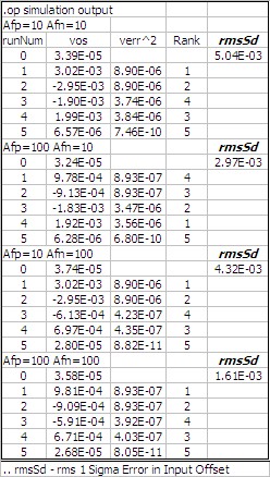
The simulation schematic, coded in LtcSpiceIV, showed a simple CMOS opamp input stage. The LtcSpice buf and inv functions are used to created a 1 sigma RMS mis-match table show below.
Mis-Match Table For RMS Evaluation
runNumber mmp1 mmp2 mmn1 mmn2 mmn3
0 0 0 0 0 0 Nominal
1 1 0 0 0 0 Input Pair 1
2 0 1 0 0 0 Input Pair 2
3 0 0 1 0 0 Current Mirror 1
4 0 0 0 1 0 Current Mirror 2
5 0 0 0 0 1 Gain Stage
The parameter ".step" function is used to generated nested loops that evaluate offset vs device gate area.
... note the LtcSpiceIV database for this example can be obtained without charge via email request.
This example demonstrates the application of RMS statistical analysis to input offset of a simple Opamp. The schematic shows the basic structure for a 4 MOSFET transconductance input stage(Input differential pair followed by current mirror).
Design Goals
Unity gain bandwidth about 2Mhz with Compensation capacitor = 1pf
4 Sigma Input Offset below 10mv
Basic Design Parameters
Maintain vgst(vgs-vt) = 100mv to guarentee strong inversion
---> Input Stage Transconductance => 12ua/v ;Miller Compensator
---> Input Pmos Devices net mw/l => 3.0
As expected the pmos matching is much more important than the nmos matching. Examination of the simulation data shows;
Afp=100,Afn=10 => 4 sigma error = 12mv
Afp=100,Afn=100 => 4 sigma error = 6mv
Re-calculating Afn for the required total offset yields an area factor of 40.
With input offset optimized, the opamp cell can be completed and characterized

kpp=67ua/v^2; kpn=206ua/v^2