

Statistical Design
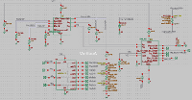
The customer, a fabless semiconductor company, was developing a mixed signal Integrated circuit for advanced power management systems. The IC was tooled in a recently introduced, fine line high voltage CMOS process. The wafer foundry supplied only a nominal simulation model for the NPN transistor used in the system voltage reference. The resistor and MOS elements simulation models were corner based. The first silicon sample reference system could not be trimmed to nominal voltage or temperature coefficient. IC Design Services was engaged to define the root causes and generate corrective action for the production version of the device.
IC Design worked with the customers engineering staff to characterize the silicon and define the root causes. Statistical simulation models(batch and random mis-match) were developed and implemented in the customers simulation environment. Design corrective actions were identified and verified in the new simulation environment. After project completion the customer was able to predict the behavior of the reference system and reduce the number of trim bits required for the reference system.
Copyright 2009 IC DESIGN SERVICES

Statistical IC Design
Yield Improvement
PDK Improvement


